Samsung first to mass produce 3-nanometer chips

Minister of Trade, Industry and Energy Lee Chang-yang, center in front row, Samsung Electronics Device Solutions Division head Kyung Kye-Hyun, second from left in the same row, and key semiconductor industry officials raise their fist to celebrate the mass production of 3-nanometer chips at the manufacturing plant of Samsung Electronics in Gyeonggi Province, Monday. Yonhap
By Lee Kyung-min
Samsung Electronics said Monday that it succeeded in mass producing 3-nanometer chips, becoming the first chipmaker to reach the milestone. The latest achievement to reduce the size and boost the power of semiconductor chips puts Samsung ahead of its global foundry rivals such as TSMC and Intel.
The achievement by the global leader in memory semiconductors is expected to cement its lead in the foundry business, underpinned and lifted by local partner firms involved in the materials, parts and equipment industries, as well as logic chips and intellectual property (IP) design, according to industry analysts.
The feat is also expected to elevate Korea's standing on the global stage via the firm's increased contribution to supply chain stabilization around the globe. This, in turn, is expected to fortify Korea's voice in determining international directives concerning the high-tech industry, pivotal in protecting the country's economic interests and bolster national security, they added.
Three-nanometer products refer to a new, improved generation of silicon semiconductor chips. Their increased transistor density helps increase speed and reduce power consumption. A nanometer is one-billionth of a meter. A human hair is about 100,000 nanometers wide.
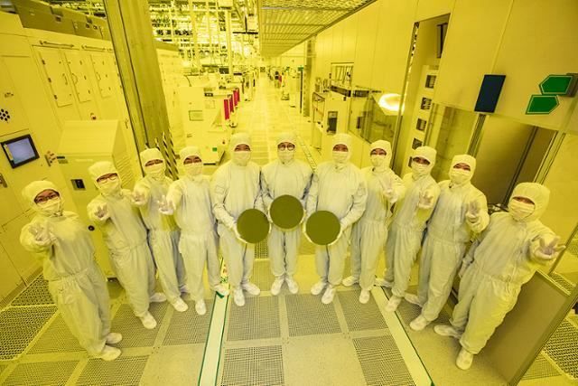
Employees at Samsung Electronics' foundry business, research and global manufacturing infrastructure oversight departments celebrate the mass production of 3-nanometer chips at the firm's manufacturing plant in Gyeonggi Province, Monday. Korea Times file
Advanced technology
The new chips use the gate-all-around (GAA) field-effect transistor (FET) technology, which is a more advanced version of the fin-shaped field-effect transistor (FinFET) technology.
Compared to FinFET, chips made using GAA technology are 50 percent more energy efficient, 30 percent more powerful and use 35 percent less space.
The new chips began rolling off the V1 Line at Samsung's Hwaseong plant in Gyeonggi Province, Monday.
Minister of Trade, Industry and Energy Lee Chang-yang attended the event to deliver his congratulatory remarks. Among some 100 attendees were Samsung Electronics Device Solutions Division head Kyung Kye-hyun and other industry leaders and officials from partner firms.
Lee vowed to provide greater assistance for the growth-driving industry.
“The government will provide tax incentives, fortify infrastructure and nurture highly-skilled semiconductor experts to sustain and spur the industry's growth momentum,” he said.
Monday's milestone was the result of five years of review of the commercial viability of the 3-nanometer technology, backed by nearly two decades of in-depth research into GAA transistor structures.
Samsung stressed that the landmark achievement in the country's semiconductor manufacturing history was the result of the firm's collaborative efforts over the past few years.
“Our foundry business, research and global manufacturing infrastructure oversight departments all worked tirelessly to overcome our limitations,” it said in a statement.
Also propelling the effort was a clear sense of responsibility among Samsung employees to turn a crisis into an opportunity, Kyung said.
“The research for the expedited development of GAA technology was driven by concerns that FinFET technology would no longer be able to meet our production needs,” he said at the event. “The new technology, in hindsight, is the definition of the pioneering spirit.”